1. Introduction
In multicolored fluorescence microscopy, pixel shift can cause imaging errors, which can lead to
erroneous interpretation of biological data [1]. This article highlights some key considerations in the
design of optical filter sets with “zero pixel shift” (less than one pixel error) performance.
2. Physics of pixel shift
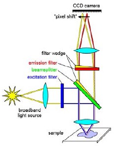
Optical filters are typically the only component in an imaging system that changes when a sequential,
composite image is created. The major imperfection in optical filters that causes pixel shift is beam
deviation created by a nonzero wedge angle (nonparallelism) of either the dichroic beamsplitter and/or
the emission filter, since both of these filters are in the imaging path (see Fig. 1). A variation in the
parallelism of filters in the filter sets associated with different colors causes the different emission beams
to be deflected by varying amounts, thereby producing a pixel shift between the different-colored portions
of the composite image (see [1] for further illustration).
Figure 1: In an epifluorescence microscope, a wedge angle on the dichroic beamsplitter or emission filter causes a beam deviation (gold path) that results in pixel shift. The wedge and beam deviation
angles are exaggerated for illustration.
The underlying physics behind pixel shift can be explained by looking at beam deviation in a wedged
piece of glass. When a beam of light travels through a glass plate with surfaces that are not perfectly
parallel, the direction of the emerging beam is deviated, or no longer parallel to that of the incident beam.
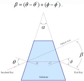
Beam deviation caused by a substrate wedge depends on the angle of incidence θ , the index of
refraction of the substrate material N, and the substrate wedge angle α . Beam deviation through a
wedged substrate is schematically illustrated in Figure 2. The total beam deviation (β) is given by
β = (θ −θ ' ) + (φ −φ ' ) . (1)
Figure 2: Beam deviation through a wedged substrate (not to scale).
Applying Snell’s law, the beam deviation can be expressed in terms of only θ , α , and N as

When θ = 0 and α is very small, the above result can also be simplified to

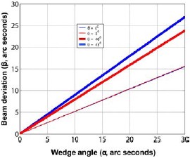
Therefore, beam deviation clearly depends upon the substrate wedge angle α and is also influenced
by the orientation of the filter with respect to the incident beam θ. However, it should be noted from
Equation 2 that for a given substrate wedge angle α, the beam deviation β is more pronounced at higher
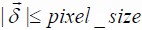
angles of incidence θ (see also Fig. 3). Since the dichroic beamsplitter is conventionally placed at a 45
degree angle, for a given substrate wedge the dichroic produces a larger beam deviation than an
emission filter does (typically placed at about a 5 degree angle).
Figure 3: Beam deviation is also sensitive to the angle of incidence of the beam
with respect to the optical filter. For a given wedge angle (α ), relatively larger
beam deviation takes place when the optical filter is placed at 45 degrees with
respect to the beam (dichroic) than when placed normal to the incident beam (emission filter).
The dependence of beam deviation on angle θ also suggests that a variation in the angle of each filter type from the ideal angle (45 degrees for dichroics and typically 5 degrees for emitters) from one
cube to another could result in a relatively large pixel shift. However, this effect is negligible since in order
for the microscope to maintain proper operation the angle of the dichroic has to be maintained fairly close
to 45 degrees, and the orientation of the emission filter has negligible impact on pixel shift (Fig. 3).
Beam deviation essentially causes the transmitted wavefront to be deviated away from the direction
of the incident wavefront’s propagation (Fig. 4). Apart from the lack of parallelism of the two opposing
surfaces of the dichroic and of the emission filter, the curvature of a filter can also impact beam deviation
(Fig. 4C). A curved dichroic beamsplitter placed in the emission path of a microscope can produce beam
deviation leading to pixel shift. For the purpose of analysis however, it can be shown that the beam
deviation due to curvature can be equivalently expressed by beam deviation due to substrate wedge.
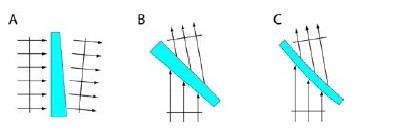
Figure 4: Substrate wedge of the emission filter (A) and the dichroic (B) as well as the substrate curvature of the dichroic (C) are the primary factors that affect
beam deviation.
Contrary to a widely accepted notion, the non-zero thickness of the dichroic beamsplitter should not introduce pixel shift in an ideal microscope using infinity-corrected objectives and a tube lens. The beam
passing through the filters is collimated, and thus the beam emerging from the dichroic, although slightly
offset laterally by an amount proportional to the thickness of the dichroic, is parallel to the incident beam.
According to first-order optics (a good approximation in this case), lateral offset in the beam path does not
create appreciable pixel shift. However, if the light transmitted through the angled dichroic is converging
or diverging, the even a perfectly parallel dichroic does cause an appreciable shift of the image on the
camera. Thus, care should be taken to avoid placing a dichroic between the tube lens and the camera.
3. Theory of designing a “zero pixel shift” filter set
In order to design a “zero pixel shift” filter set, the beam deviation resulting from wedge error should
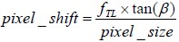
be related to the amount of pixel shift. In a CCD camera, pixel shift in the image plane is described by:
where pixel _ shift is the shift in the number of pixels, β is the net beam deviation from the dichroic and emitter pair,
fTL is the focal length of the tube lens, and
pixel _ size is the center-to-center pixel
spacing of the CCD camera.
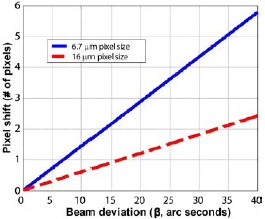
Figure 5: Impact of beam deviation on pixel shift. Blue curve assumes fTL=200mm and pixel_size =6.7µm whereas red (dotted) curve assumes pixel_size = 16µm.
For a microscope with a 200mm focal length tube lens and a CCD camera with pixel size of 6.7μm, a net beam deviation of 6.9 arc seconds causes a total pixel shift of one pixel (based on Eq. 2). Thus an
example of “zero pixel shift” specification is the requirement that the net beam deviation from the filter set
be less than 6.9 arc seconds. For some cameras, however, the size of a pixel may be much larger than
6.7μm, or the effective pixel size may be larger due to binning, and therefore the requirements may be
much less stringent (see Fig. 5).
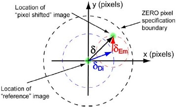
Figure 6: Design principle of a “zero pixel shift” filter set is illustrated with the image location of a point source. Pixel shift
 is the vector sum of the pixel shifts
 and ,
and ,
 the individual contributions for pixel shift by dichroic and emitter respectively. In order to obtain
“zero pixel shift” performance,
the individual contributions for pixel shift by dichroic and emitter respectively. In order to obtain
“zero pixel shift” performance,
 .
.
The term “pixel shift” only makes sense when defined relative to a reference image point. In fluorescence microscopy, typically any one of a group of single-colored fluorescence images is
considered the reference image. Therefore, in order to obtain “zero pixel shift” performance, it is sufficient
that the location of the pixel-shifted image of a point source (e.g., the green dot away from the origin in
Fig. 6) does not shift by more than one pixel relative to the location of the reference image (green dot at
the origin in Fig. 6). As illustrated in Figure 6, Semrock’s “zero pixel shift” specification boundary
corresponds to a circle of one pixel radius (see also Section 5). Mathematically, this criterion can be
expressed as:
where
Here
is a vector that represents the net pixel shift, which is comprised of the individual dichroic and
emitter contributions,
and , respectively. Since the wedge directions as well as the filters
themselves can be randomly oriented in a filter cube, the individual contributions to pixel shift could either
intensify or even nullify the net shift, and hence a vector addition is required.
4. Manufacturing a “zero pixel shift” filter set
Due to the limitations of the traditional filter manufacturing techniques, such as soft-coated filter
technology based on e-beam or thermal evaporation, it was difficult to make “zero pixel shift” filter sets.
Because the emitter was based on multiple substrates laminated together (Fig. 7A), it was nearly
impossible to achieve a low wedge angle without expensive post-processing of the finished filter. Emitter
and dichroic filter pairs with similar beam deviations had to be hand-selected, and subsequently the filters
were carefully oriented with respect to one another in a filter cube so that the beam deviations of the two
filters canceled (Fig. 7B).
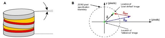
Figure 7: Manufacturing a “zero pixel shift” filter set using soft-coating technology. Since the wedge angles of the dichroic and the emitter are fairly large (and difficult to control) as shown in (A), careful “relative orientation” of the
dichroic and a matching emission filter needs to be maintained in order to achieve “zero pixel shift” performance (B).
Furthermore, once carefully aligned, the filters could not be removed from the cube or replaced except by the filter vendor. This approach for correcting the pixel shift error is primarily dictated by the
limitations of the manufacturing process itself since it is difficult to control the wedge angle in multisubstrate
thin-film optical filers. Another implication of the poor control of the wedge-angle in soft-coated
filters is that non-”zero pixel shift” filter sets can account for several pixels of error.
Figure 8: Manufacturing a “zero pixel shift” filter set using Semrock’s Ion Beam Sputtering hard-coating technology. Since the wedge angles of the dichroic and the emitter are small and easy to control, as shown in (A), “zero pixel
shift” performance can easily be obtained by simply matching a dichroic and emitter pair that provides less than one
pixel error (B).
With the advent of modern hard-coated fluorescence filter technology, such as the Ion Beam Sputtering (IBS) technique pioneered by Semrock, it became possible to manufacture every filter with a
single substrate (Fig. 8A), therefore ensuring a small wedge angle of the filters simply by starting with
high-quality substrates prior to deposition of the optical coatings. Since the beam deviations associated
with hard-coated dichroics and emitters are much smaller than those of soft-coated filters, it is possible to
achieve “zero pixel shift” specifications without having to carefully match the orientations of the dichroics
and the emitters (Fig. 8B). Hence, no special alignment or assembly are required to install the filters in a
cube, and a microscope user can populate his or her own cubes and exchange filters as often as desired.
5. Discussion
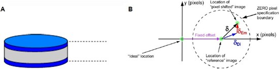
As discussed above, in fluorescence microscopy a “zero pixel shift” filter specification generally
means that no appreciable pixel shift should be observed among the images acquired from different
fluorophores when using different filter cubes for different colors. However, a “zero pixel shift”
specification might not necessarily imply no appreciable pixel shift between the fluorescence images and
a brightfield image, or one acquired with no fluorescence filters in the emission path (denoted as the
“ideal location” of the image in Fig. 8B).
Since the intrinsic stress of the thin-film coatings in a hard-coated filter can be different from that of
the substrate, a slight bending (or curvature) of the substrate may result. This curvature is particularly an
issue for the dichroic, and it produces a beam deviation and resulting pixel shift that is always along the
same direction on the CCD camera. As alluded to above, this “fixed offset” in Fig. 8B due to the dichroic
bending is present in all standard hard-coated filters, unless specifically compensated for. While it is
possible to “flatten” the dichroic (i.e., undo the bending) by applying an additional balancing coating on
the opposite face of the dichroic, this approach results in an appreciable cost increase. In order to provide
the most cost-effective solution, Semrock’s “zero pixel shift” specification boundary is defined with respect
to the location of the reference image, which is offset from the origin (“ideal location” in Figure 8B) by a
distance denoted by “fixed offset” in Figure 8B. The direction of this vector is always fixed (i.e., known)
since the orientation of the coated and reflecting surface of the dichroic is known. Also, since Semrock’s
manufacturing process is highly repeatable, the length of this vector is held constant to a very high
tolerance for all of the standard, high-performance single-band dichroics.
Note that it is still possible to obtain “zero pixel shift” performance when doing simultaneous
fluorescence and brightfield imaging by matching the beam deviation in the brightfield imaging path with
the beam deviation in the fluorescence imaging light path. This matching can be done with a special
brightfield “zero pixel shift” filter cube that is introduced in the transmission path of brightfield imaging (see
the Semrock BRFLD-A-000-ZERO set).
Since the design approach for a “zero pixel shift” filter set can be different based on the different
manufacturing techniques, “zero pixel shift” filter sets from different manufacturers are typically not
compatible with one another. For example, the “standard offset” might be different for different
manufacturers. Therefore, software-based pixel-shift correction might be required when filter sets from
different manufacturers are used together.
Imperfections in the filter cube assembly also contribute to pixel shift to some extent. In general, this
effect is not significant enough to produce noticeable pixel shift when the cube is assembled correctly.
Nevertheless, a margin of error for the cube assembly is taken into account in determining the “zero pixel
shift” specification boundary (Section 3).
In high-volume manufacturing, specifications are usually generated based on a statistical sampling of
large numbers of components. For example, the location of the reference image in Figure 8B corresponds
to the location of the mean of the “pixel shifted” image locations of a significantly large number of
Semrock filters. By studying Fig. 8B, one can see that it is theoretically possible that “zero pixel shift” filter
sets can result in more than one pixel (even up to two pixels) relative error. However, the probability of
this error is very low, since it occurs only when the vectors for two cubes are pointing exactly opposite
each other and are of exactly equal length. Therefore, selection of a “zero pixel shift” specification
boundary (in Figs. 6 and 8) of only half a pixel would essentially be an overdesign considering the
statistical manufacturing variability.
Finally, any design is only as good as its underlying assumptions. This principle also applies to the
design of “zero pixel shift” filter sets. For example, Semrock’s “zero pixel shift” filter sets assume a
detector pixel spacing of 6.7 μm, and a 200 mm focal length tube lens. These assumptions are based
upon the fact that a significant percentage of the popular (and high-end) imaging systems have
specifications similar to these. But as Eq. (3) demonstrates, significantly different values of the pixel
spacing and tube lens focal length in any given microscope configuration will result in a different number
of pixels (or fraction of a pixel) associated with an image shift.
6. References
Authors
Prashant Prabhat, Ph.D. and Turan Erdogan, Ph.D.